CHEM-E4175 - Fundamental Electrochemistry, 09.01.2019-18.02.2019
This course space end date is set to 18.02.2019 Search Courses: CHEM-E4175
Kirja
5. Electrical double layer and adsorption
In electrochemical reactions, there is always an electron transfer step, which takes place at the interface of two phases, for example at the interface of an electrode and electrolyte solution. This interface is studied in greater detail in this chapter.
At the interface of the two phases, there is an interfacial zone, the properties of which are significantly different from those of the inner part of the phase. From an electrochemical point of view, it is important to note that the electrical properties of the interface also differ from those of the bulk phase. If the interfacial region carries a charge, the charge concentrates at the interface. The orientation of the dipole molecules at the interface can also have an effect on the electrical properties of the interface. Furthermore, the adsorption of the dipole molecules or ions on the interface can enhance the accumulation of charges. This charge excess is due to the electrons, ions and dipoles, and generates an electric field. The region in which the charges are located is called the double layer.
When oppositely charged ions and dipoles accumulate on the surface of a charged electrode in an electrolyte solution, a double layer as depicted in Figure 5.1 is formed. The surface properties of the electrode differ from those of the inner phase of the electrode because of the charge excess or deficit with respect to the bulk of the electrode. This interfacial zone on both sides of the phase boundary is called the electrical double layer.
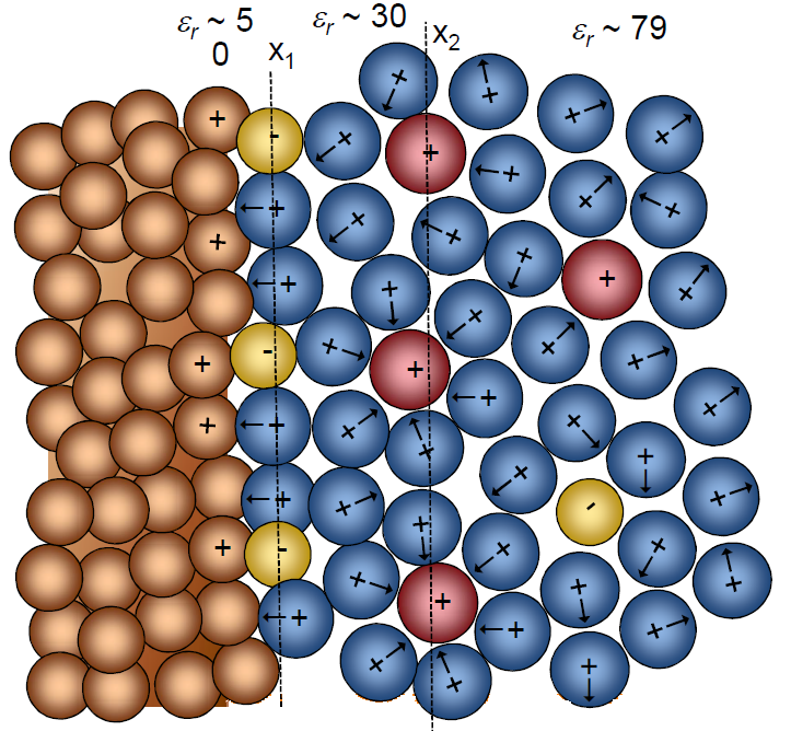
Figure 5.1. Structure of an electrical double layer in an electrolyte solution, when the solution is in contact with a charged electrode. The ions with the solvation layer are closest to the interface at the outer Helmholtz layer (x2), whereas the specifically adsorbed ions at the inner Helmholtz layer (x1) are desolvated.
The solution in the region of the double layer is thought to be made up of several layers. The structure of these layers is affected by the finite size of the ions and molecules, electrostatic forces, mixing entropy, and thermal motion, which reduces the level of organization of the species. The layer closest to the interface is called the inner Helmholtz plane (Figure 5.1). The inner Helmholtz plane consists of specifically adsorbed molecules and ions. Species that are specifically adsorbed are affected by not only electrostatic interactions but also chemical interactions between the surface and the species. The specifically adsorbed species are typically anions, solvent molecules or other neutral molecules. Cations, on the other hand, are very seldom specifically adsorbed. The inner Helmhotz plane is located at the electrical centers of the specifically adsorbed ions.
The outer Helmholtz plane (OHP) is thought to be located at the electrical centers of the closest solvated ions near to the electrode surface. These ions are said to be nonspecifically adsorbed, and the interaction of the solvated ions with charged metal surface involves only long-range electrostatic forces. Their interaction is therefore in principle independent of the chemical properties of the ions.
The region extending from the outer Helmholtz plane to the bulk of the solution is called the diffuse double layer, where the species are organized by thermal motion and the electrostatic force, which gets weaker as the distance from the interface increases. The boundary between the diffuse layer and the bulk of the solution is therefore not well defined. The thickness of the diffuse layer depends on the total ionic strength and is of the order of magnitude10-100 \( \mu \)m.
 |
a |
|---|---|
 |
b |
 |
c |
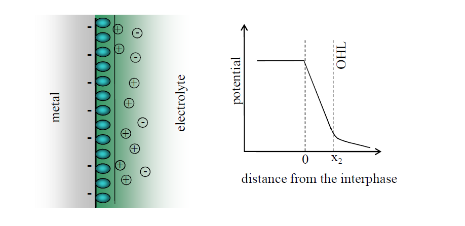
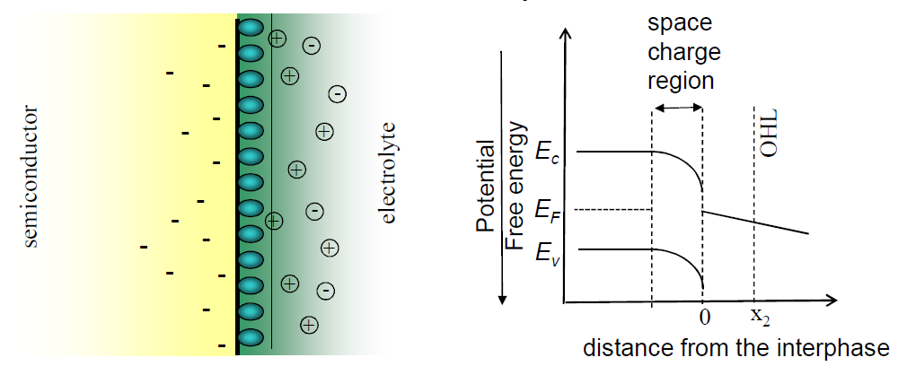
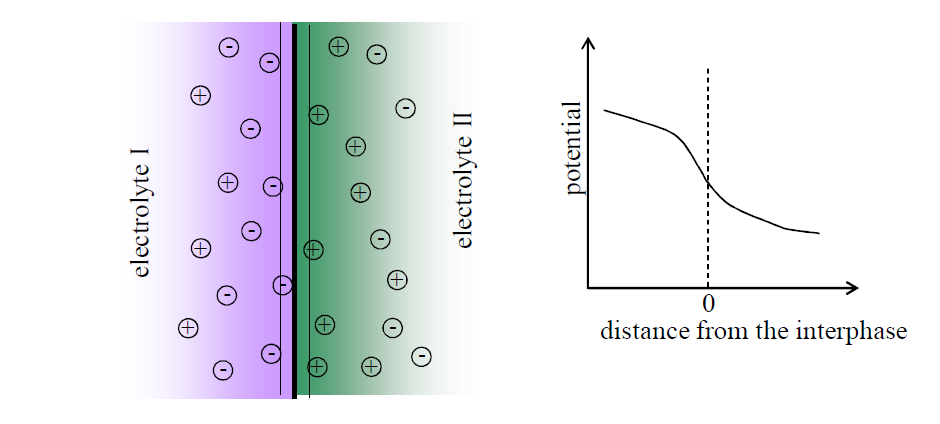
Figure 5.2. Structure of electrical double layer and potential distribution at a) the metal electrode-electrolyte interface, b) the semiconductor-electrolyte interface, and c) the interface of two immiscible electrolyte solutions without specifically adsorbed species. Note that in the latter case there is no layer of organized solvent ions at the interface, according to Verwey and Niessen model.
The structure of the electrical double layer and the potential distribution at a) the metal electrode-electrolyte interface, b) the semiconductor-electrolyte interface, and c) the interface of two immiscible electrolyte solutions without specifically adsorbed species is shown in Figure 5.2. At the surface of a semiconductor, the charges are distributed more widely compared to the surface of a metal electrode. At the interface of two immiscible liquids, there is no layer of organized solvent molecules.